ICCAD 2017 Contest
Power Distribution Network Optimization
Yung-Tai Chang, Yow-Tyng Nieh, Industrial Technology Research Institute
0. Announcements
- FAQ Updated - 2017-09-05
- FAQ Updated - 2017-08-28
- New TestCase released - 2017-08-21
- Beta Test Result Announcement - 2017-08-17
- FAQ Updated - 2017-08-02
- FAQ Updated - 2017-07-21
- FAQ Updated - 2017-07-17
- FAQ Updated - 2017-07-10
- FAQ Updated - 2017-07-06
- FAQ Updated - 2017-07-04
- DRC verification guideline released - 2017/06/27
- FAQ Updated - 2017-06-13
- FAQ Updated - 2017-06-08
- Content Updated - 2017-06-08
- FAQ Updated - 2017-06-01
- TestCase Updated - 2017-05-31
- FAQ Updated - 2017-05-12
- FAQ Updated - 2017-05-10
- FAQ Updated - 2017-05-08
- New testcase released - 2017/04/19
- FAQ Updated - 2017-03-21
- New testcase released - 2017/03/20
- FAQ Updated - 2017-03-08
I. INTRODUCTION
A power distribution network (PDN) delivers current from power sources to all devices (including standard cells and hard IPs). As the process shrinks into the deep sub-micron technology, higher chip frequency and increasing power consumption may cause fluctuation of power supply levels and lead to design failure. A robust PDN is essential to ensure reliable circuit operations on a chip. In this problem, given an initial PDN, the contestants have to optimize the power routing with minimum routing resource while satisfying all specified IR-drop constraints.
To reduce the voltage drop, the PDN optimization techniques include wire sizing, wire movement and wire density increment. In addition to these techniques, the contestants are also allowed to re-design or modify the given power routing, resulting in a routing topology, which is different from the initial PDN.

Fig.1 Netlist and floorplan of a PDN.
Figure 1 shows the netlist and its initial floorplan of a PDN. There are three hard IPs, B1, B2, and B3, and three power sources, VDD1, VDD2, and VDD3. Each power source is connected to some power pins on different hard IPs, where VDD1 is connected to VDD_A/B1, VDD2 is connected to VDD_B/B1, and VDD3 is connected to both VDD_A/B2 and VDD_A/B3. Each power net can be routed with horizontal and vertical metal wires. A metal via must be applied when connecting different metal layers. The usage of upper metal layers is more preferable because of smaller resistance and capacitance.

Fig.2 Initial power routing.
Figure 2 shows an example of the initial power routing of the PDN. In this example, both horizontal and vertical metal wires in each metal layer can be used for routing power nets. Note that, a hard IP may only employ a certain number of lower metal layers for its internal routing. Hence, upper metal layers, which are not used by hard IPs, can also be used for routing over the underlying hard IPs.

Fig.3 PDN optimization.
An optimized power routing result is given in Figure 3 based on the following procedure: First of all, we widen the power net from VDD1 to B1/VDD_A in order to satisfy the IR-drop constraint. Then, we shorten the length of the power net from VDD2 to B1/VDD_B. In this example, B3 only contains the layers of Metal 1 to Metal 5, so we can route over B3 with Metal 6 for shorter wire length. Finally, we split the horizontal wires on Metal 6 from VDD3 to B2/VDD_A into three parallel wires. As a result, the resistance of these power wires is nearly threefold reduction, and hence the IR-drop constraint can be satisfied.
The contestants have to produce a power routing result with minimized usage of routing resources. The final routing solution should meet the voltage drop constraints at each power pin of all hard IPs. The NGSPICE software is provided to calculate the voltage drop at each power pin.
II. Problem Description
The problem is given the following inputs:
- A Verilog netlist file of a design;
- A DEF (Design Exchange Format) file specifying an initial floorplan of hard IPs and the initial power routing;
- LEF (Library Exchange Format) files specifying design rules and abstracted information of each hard IP;
- A file specifying the current drawn by each power pin.
- A file specifying the voltage of each power source.
- A file specifying IR-drop constraints.
- A file containing a weight for each metal layer.
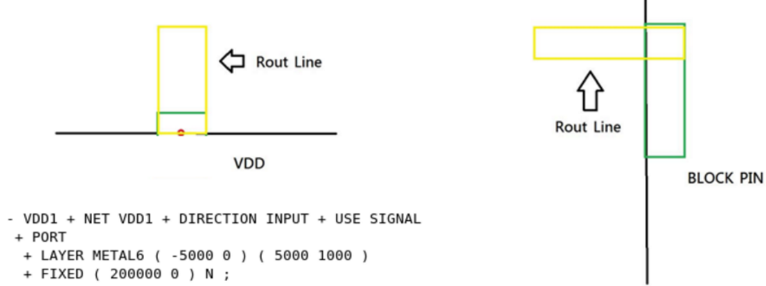
A program must be developed to read/write a DEF file that contains the actual layout including metal wires and vias. It must also generate some other information given in Section 4. Figure 4 shows an output DEF file which describes a power routing solution to the problem given in Figure 3. Note that the dimensions of metal vias can be found in the given LEF file (tech.lef).

Fig.4 An output DEF file for a routing solution.
A LEF (tech.lef) file contains information about resistance per square of metal wires and vias. The resistance of a metal wire on layer N can be calculated by the following equation:
$R_{MetalN}=R_{PeerSq} \times \frac{Metal\ Length}{Metal\ Width}$
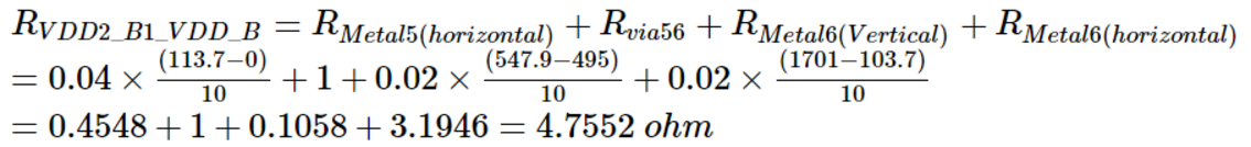
An example of the total resistance of the power net from VDD2 to B1/VDD_B is calculated as follows:
$R_{VDD2\_B1\_VDD\_B}=R_{Metal5(horizontal)}+R_{via56}+R_{Metal6(Vertical)}+R_{Metal6(horizontal)}$
$=0.04 \times \frac{(113.7-0)}{10} + 1 + 0.02 \times \frac{(547.9-495)}{10} + 0.02 \times \frac{(1701-103.7)}{10}$
$=0.4548+1+0.1058+3.1946=4.7552\ ohm$
Suppose the voltage of all power sources is 1.0V. According to the calculated resistances, as shown in Figure 5, the contestants further need to generate a SPICE netlist for IR-drop simulation using the NGSPICE circuit simulator. Figure 6 shows the SPICE netlist for the circuits in Figure 5.

Fig.5 Circuit networks for an optimized power routing solution.

Fig.6 SPICE netlist for the circuits in Figure 5.
We will also provide a binary executable NGSPICE for LINUX environment (as seen the attached file ngspice_26_linux.tgz) for IR-drop simulation. The source code of NGSPICE can be downloaded from the website below.
http://sourceforge.net/projects/ngspice/files/ng-spice-rework/26/
We encourage the contestants to embed the source code into their programs.
III. Inputs
The inputs to the problems given in Figure 1 are detailed below.
- Verilog netlist
A Verilog netlist consists of a hierarchy of modules, connections between power sources and power pins of hard IPs. (As the attached file case1.v) -
DEF file
An initial DEF file gives the chip size and locations of all power sources and hard IPs. (As the attached file case1_initial.def) -
LEF files
There are two LEF files, tech.lef and blocks.lef, for this problem. The tech.lef gives the resistance per square on each metal layer, the range of wire width, and via size/resistance. The blocks.lef describes the shapes of hard IPs, power pin locations, and the blockages of hard IPs. (As the attached files tech.lef and blocks.lef) -
The current drawn by each power pin
# The current drawn by each power pin (mA)
B1 VDD_A 5
B1 VDD_B 2
B2 VDD_A 3
B3 VDD_A 2
-
The voltage of each power source
# The voltage of each power source (V)
VDD1 1.0
VDD2 1.0
VDD3 1.0
-
IR-drop constraints (in % of the related power source voltage)
# The IR-drop constraint of each power pin (%)
B1 VDD_A 1
B1 VDD_B 1
B2 VDD_A 1.8
B3 VDD_A 1.5
-
The weights on metal layers
# The weights on metal layers
M1 2.49
M2 2.07
M3 1.73
M4 1.44
M5 1.20
M6 1
IV. Outputs
The output files for a solution to the problem in Figure 1 are as follows.
- DEF file
As seen in the attached file “case1_output.def”. -
A metal usage report file
The contestants can calculate the metal usage of a routing solution as follows:
$Metal\ usage = \sum\limits_{n=1}^N(Total\ Metal\ Area)_{Metal\ n} \times Weight_{Metal\ n}$
Where N is the number of metal layers used for power routing of hard IPs.
# The metal usage report
M5 11881
M6 100770
Total 115027.2
-
SPICE netlist
As seen in the attached file “case1.sp”, which contains the circuit description for a routing solution. -
Voltage drop report
The contestants should employ the following commands to report the voltage at each node for a routing solution based on the NGSPICE simulation.source case1.sp
run
quitFigure 7 shows the voltage result after NGSPICE simulation.

Fig.7 A voltage report at each node.
The final report that gives IR-drops is shown below (in % of the related power source voltage):
# The IR drop of each power pin (%)
B1/VDD_A 0.96
B1/VDD_B 0.95
B2/VDD_A 1.65
B3/VDD_A 1.21
V. Evaluation
Evaluation priority:
- All the output files are correct.(especially DEF file)
- The output DEF file can’t have DRC (Design Rule Check) error.
- The voltage drop of each power pin cannot exceed its IR-drop constraint.
- Minimization of the whole metal usage.
- Run time.
| Case1 | Case2 | Case3 | Score | Ranking | |||||||
| DEF pass 0% | No DRC 30% | Meet IR 70% | DEF pass 0% | No DRC 30% | Meet IR 70% | DEF pass 0% | No DRC 30% | Meet IR 70% | |||
| CAD01 | ○ | ○ | ○ | ○ | ○ | ╳ | ╳ | -- | -- | 33+33*30%=42.9 | 1 |
| CAD02 | ○ | ○ | ○ | ○ | ╳ | -- | ○ | ╳ | -- | 33 | 2 |
| CAD03 | ○ | ○ | ╳ | ○ | ○ | ╳ | ○ | ○ | ╳ | 3*(33*30%)=29.7 | 3 |
An evaluation example is given in Table 1, where Case1 to Case3 are test cases. We evaluate the correctness of DEF files, correctness of DRC, and satisfaction of IR-drop constraints in sequence. Note that, if an output DEF file has syntax errors or DRC errors, we will not evaluate the IR-drop constraints anymore. A team can’t get any score for this benchmark circuit. In addition, if more than one team receives the same score, we will check the metal usage report (priority 4) and program runtime (priority 5) to decide the ranking.
Physical guideline:
- Metal wires used for routing different power nets can not be shorted, as shown below.

- Minimum and maximum wire width of each metal layer are given in tech.lef.
- Every two metal wires on a layer must follow the spacing rules in tech.lef.
- Two hard IPs may abut (i.e. spacing is 0). The spacing rules between metal wires and hard IPs are the same as that given in guideline 3.

-
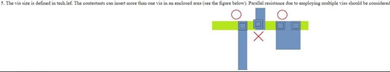
The via size is defined in tech.lef. The contestants can insert more than one via in an enclosed area (see the figure below). Parallel resistance due to employing multiple vias should be considered.

-
When the total metal area of a bent wire is calculated, the overlapped area at corners should not be counted repeatedly.

VI. TestCase
- testcase1
- testcase2 - 2017/05/31
Release_0419說明如下
- 公布case2相關檔案,包括blocks.lef case2_input.def case2.v initial_files tech.lef
- 公布DRC驗證流程相關檔案, 包括說明檔Innovus_DRC.pdf與ProblemE_test目錄
- 若要進行DRC驗證 , 輸入的.def檔案需有完整的Design資訊, 不能只讀入SPECIALNETS的資訊.因此請參照更新後的case1_output.def來進行DRC驗證
- 更新case1與case2測試範例中的tech.lef, 其中METAL 6部分PITCH 值改為3
-
因CIC環境無Innovus軟體, 故改用Cadence encounter軟體來驗證DRC. 同步更新說明檔(encounter_DRC.pdf)
-
程式執行時讀入/寫出檔案的順序需統一如下:
假設執行檔為cadb001,要執行case1測試檔,程式執行指令應該為:
cadb001 case1.v case1_input.def tech.lef blocks.lef initial_files case1_output.def case1.sp output_files - testcase3 - 2017/08/21
testcase3 Floorplan image
內有三個initial_file, 請參賽者依序執行
參賽者亦可更動initial_file 來自我測試程式
未來部分隱藏測試檔有可能只是更改initial_file條件來做測試
VII. Alpha Test
目前只有三組寫出與input def一樣的輸出結果,請大家繼續努力!
VIII. Beta Test

XIV. FAQ
- 我們在官網上有看到說他的Benchmark解釋有附一個網址 http://projects.si2.org/openeda.si2.org/projects/lefdef,這個是用來轉和 lef 跟 def 檔的嗎? 請問詳細的 Benchmark 解釋的 PDF 檔何時會釋出? 還是正式的 Benchmark 都是等報名完才會陸續釋出?
去年的Q&A所附的網址,僅用來讓同學查詢LEF跟DEF檔案的定義,並不是用來當LEF跟DEF檔的parser。至於Benchmark 的解釋,如果同學有不懂的地方,可以在Q&A中詢問,Benchmark Case1會在近期內釋出。 - 要如何在makefile裡執行NGSPICE 並同時將其資料回傳到program裡做運算產生outputfile呢?
並不是在makefile 執行NGSPICE,而是程式要呼叫NGSPICE進行運算,請參考2016 Q&A 15以及 Q&A 27說明。 - 3. 想要知道有關去年problemE裡的CASE1中 B1_VDDA -> VDD1:其座標分別是(1696,354)(200,0)。假設不管OBS且以Maxwidth最佳解做計算 (1696-200)*0.04/10 + (354-0)*0.02/20+1=7.338Ohm,乘上0.005A 得到IR_DROP是0.03669,約為3.67%。如果要符合LAYER限制這斯呼是不太可能的。想請問這部分是學生對題目有理解錯誤還是有什麼狀況呢(B1_VDDB->VDD2也有相同狀況)?
請參考去年題目Fig.2,注意題目中VDD1 to B1/VDDA 全部都用Metal 6繞線,並請參考 2016 Q&A 1。 - 想請問一下 Rout Line接出道VDD 是只要碰到其中點就好還是要將其填滿呢(如圖)?
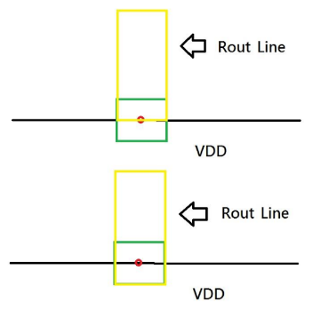
舉例case1_input.def, VDD1 power pin在DEF定義中並不會超過design boundary,因此只要連到有design boundary的部分就好,(你原本的圖超過design boundary)
-
Block Pin 有一定的範圍,這是指在這區域裡只要連接到都可以嗎(如圖)?
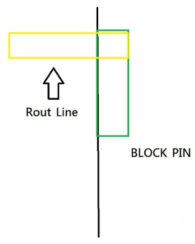
是的,我們之後會提供Cadence INNOVUS DRC驗證流程,基本上有通過其驗證即可。 -
關於 Problem E 介紹中的電阻算法,Metal length 皆是以每條線的邊界來計算,但這樣算下來,若是同一層線的轉彎處(vertical 跟horizontal重疊的部分),會多算一次!
在本年度的題目當中,為了讓參賽同學可以更容易的計算(直接使用DEF上的資訊),所以我們在計算繞線電阻值時候,其繞線在轉彎處重疊的部分可以重複計算繞線面積一次(不必像去年一樣要取中點),以下提供在題目裡,Fig.5 內VDD3到 B2/VDD_A,其中並聯電路的計算式子,如下圖所示:
另外在Output file 之metal usage report中,routing area的計算仍須扣掉轉彎處重疊的部分,若重複計算會造成較大的metal usage,請參賽同學特別注意。 -
在problem E中block.lef有給symmetry,所以在本題的實做中可以更改block的擺放方向嗎?例如從N改為S?
不行 -
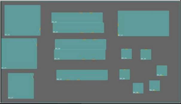
我想請問一下case2其中的Component,B2_01 block2 + FIXED ( 0 665600 ) S tech.lef中 block2的為 SIZE 700 BY 600 , 這樣在計算位置時,會超出design boundary ,同樣的情形在B2_02 B3_01 B5_03 也會發生。這部分是否有誤,還是我理解錯誤?
Def針對每個block的描述中,最後有個英文字母代表他翻轉的方向, 經過翻轉後是不會超出範圍的,旋轉說明: http://www.ispd.cc/contests/14/web/doc/lefdefref.pdf , page 186 Case2的FloorPlan應如下圖所示:
-
您好,在去年的Q&A中有說明如何產生電壓檔案,請問在我們繳交的sp檔案中可以包含如下指令嗎?還是必須要去除?謝謝
繳交的.sp檔案請去除ngspice指令 -
請問除了目前在def,lef中給的design rule,之後還會給其他design rule或DRC相關資訊嗎?
不會 -
CASE2的initial_files測資有誤:
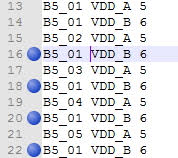
Case2 initial_files檔案的內容請更新如下
# The current drawn by each power pin (mA)
B1_01 VDD_A 5
B1_01 VDD_B 2
B2_01 VDD_A 4
B2_02 VDD_A 4
B3_01 VDD_A 10
B4_01 VDD_A 3
B4_02 VDD_A 3
B4_03 VDD_A 4
B4_04 VDD_A 4
B4_05 VDD_A 5
B4_06 VDD_A 5
B5_01 VDD_A 5
B5_01 VDD_B 6
B5_02 VDD_A 5
B5_02 VDD_B 6
B5_03 VDD_A 5
B5_03 VDD_B 6
B5_04 VDD_A 5
B5_04 VDD_B 6
B5_05 VDD_A 5
B5_05 VDD_B 6
# The voltage of each power source (V)
VDD1 1.0
VDD2 1.2
VDD3 1.0
VDD4 1.4
VDD5 1.0
VDD6 1.6
# The IR-drop constraint of each power pin (%)
B1_01 VDD_A 5
B1_01 VDD_B 5
B2_01 VDD_A 5
B2_02 VDD_A 5
B3_01 VDD_A 3
B4_01 VDD_A 5
B4_02 VDD_A 5
B4_03 VDD_A 5
B4_04 VDD_A 5
B4_05 VDD_A 5
B4_06 VDD_A 5
B5_01 VDD_A 5
B5_01 VDD_B 5
B5_02 VDD_A 5
B5_02 VDD_B 5
B5_03 VDD_A 5
B5_03 VDD_B 5
B5_04 VDD_A 5
B5_04 VDD_B 5
B5_05 VDD_A 5
B5_05 VDD_B 5
# The weights on metal layers
M1 2.49
M2 2.07
M3 1.73
M4 1.44
M5 1.20
M6 1 -
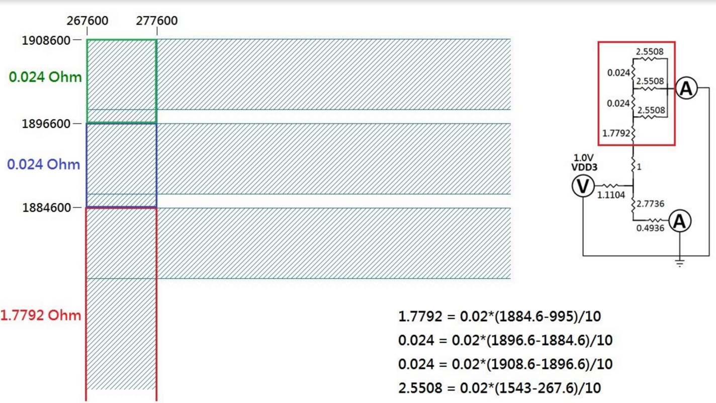
我想請問關於Problem E的metal的計算方式,我們使用題目給的公式手動計算結果跟題目範例有誤差(有扣除重疊):
M5 = 14257.2 範例=11700
M6 = 100770 範例=100800
不知道是不是學生計算的方式錯誤(附檔是M5的計算過程),請問可否給我們一份計算範例?
你對於M5 metal usage算出的結果11881是正確的,但在M5 report中應該直接report出11881,在Total結果時再乘上權重1.2,
$Total=11881 \times 1.2+100770 = 115027.2$
Ex:
# The metal usage report
M5 11881
M6 100770
Total 115027.2
在程式驗證過程中, 由於我們使用encounter report中 metal density(0.13%)來換算metal usage,因此得到的結果 3000*3000*0.13%=11700,也許跟實際結果會一點差距,但這都在誤差範圍內,不至影響驗證的結果。 -
在 case1_output.def 裡,第 56 行 NEW METAL5 10000 + SHAPE STRIPE ( 272600 311600 ) ( * 1005000 ) 的 wire 是從下到上,但是 Fig.3 裡是從上到下,我想請問這裡是不是有打反呢? 上到下應該是 NEW METAL5 10000 + SHAPE STRIPE ( 272600 1005000 ) ( * 311600 )。
這是用一塊Metal來描述一個線段,沒有方向性。 -
請問在這一題中會有多個PowerPin連到同一個BlockPin的情況嗎?
會。 -
在def的specialnet定義中,例如case1: VDD2 ( * VDD_B ),請問這個*是指同上一個嗎?(如附圖)因為在case2中沒有這樣的情況(如附圖),還是學生理解錯誤了?
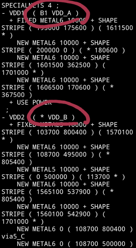
連線關係請參照netlist: block1 B1 ( .VDD_A(VDD1), .VDD_B(VDD2) ); Case1的vdd2連到B1的VDD_B pin, Def的定義請參照以下網址:
http://projects.si2.org/openeda.si2.org/projects/lefdef -
我想請問在這題中最後一個評分標準是Run time,那有time limit嗎?
基於測試程式的時效問題,我們對於程式的run time希望在十小時以內。 -
我想請問problem E還會在公佈新的測資嗎?另外想請問會有隱藏測資嗎?
再公布case3,會有隱藏測試範例,另外, 參賽者亦可可自行設計/變更input DEF 檔案來測試自己的程式。 -
請問比賽有限制最多可用幾個thread嗎?
沒有限制最多可以用幾個thread,我們會統一在同一台CIC提供的機器執行。 -
我想請問一下,metal的層數,在後面的case裡面,有可能會到兩位數,也就是>=10嗎?
不會。 -
在alpha test官網裡面寫說,只有三組寫出跟input.def一樣的輸出結果,這句話是什麼意思我有點不了解,這個input檔案不是只是一個initial PDN嗎?
以case1為例, 三組寫出來的case1_output.def 跟initial PDN(case1_input.def)是一樣的。 -
再題目裡面說的可以re-design是指說像case2裡面有許多標註為placed類型的block可以重新排列的意思嗎?
題目的意思是說, 如果參賽者覺得initial PDN(case*_input.def) 不好, 導致最佳化的結果不夠好,參賽者可以自行re-design 一個新的PDN, 不用基於原有initial PDN進行最佳化,而所有block都不可以重新排列。 -
我想請問在本題中繞線寬度需在maxwidth限制內嗎?
是。 -
根據physical guideline第2點,如果超過maxwidth也是合法的解嗎?
單條metal的寬度不可以超過maxwidth。 -
re-design一個新的PDN就是按照case1.v裡面的規格直接自己重新連線,或者是可以直接修改initial PDN這樣,所以case1_input.def裡面,若是要自行re-design的話,是可以不用讀SPECIALNETS的部分,是這個意思嗎?
是的,只要訊號連線關係跟case1.v所定義的一樣,可以不參考SPECIALNETS的部分(case1_input.def)。 -
在case2_input.def裡面那個不論是PLACED或是FIXED都不能移動嗎?那麼那個PLACED或是FIXED代表著什麼意思呢?
PLACED或是FIXED 代表此block的屬性,tool會依據此屬性來進行APR步驟,若有疑問請自行參考def格式定義,http://projects.si2.org/openeda.si2.org/projects/lefdef,本次題目皆不允許block變動位置方向。 -
請問我們應該如何驗證自己產生sp檔案內容是否正確?像是output.def可以用encounter來驗證,那有辦法驗證sp嗎?還是需要靠我們自己手驗證動?
如果.sp語法錯誤, 則容易導致電路斷路(open),ngspice會產生出很奇怪的IR-drop結果,而電壓電流電阻的計算數值, 請參賽者自行驗證。 -
在大會提供給我們的alpha test結果中,有提到一項LVS,我想請問是否是有一套LVS的驗證程序提供給我們測試spice結果是否正確呢?
LVS的驗證程序包括在encounter_DRC.pdf中的”驗證 Connectivity 結果”,因此只要你執行run_case*.tcl (裡面path要對),若所有violation數目為零就代表通過DRC/LVS 驗證。 -
在guideline的第五點有寫,Parallel resistance due to employing multiple vias should be considered,那這個的resistance有寫在哪個檔案裡面嗎,在那些檔案裏面我沒有找到相關的資訊?
題目意思是說, 單顆via的電阻值假設是1 ohm,在線寬允許的條件之下, 如果接了兩顆via,則電阻值減半為0.5 ohm,各metal間的via電阻值在tech.lef中都可查詢得到。 -
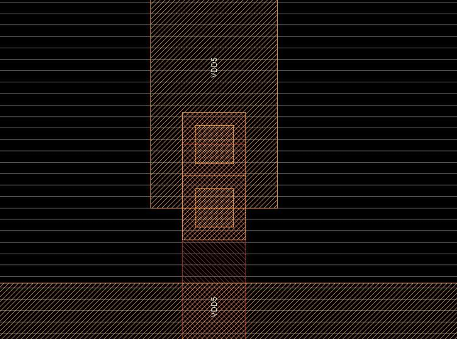
我想請問在本題中關於metal包覆via,如附圖這樣是合法的嗎?因為我們跑.tcl用encounter驗證是通過的。
請參照題目中,Physical guideline的第五點,這樣並不符合規範。
-
請問最後繳交結果,主辦方驗證DRC是使用現在提供的同一套tcl 驗證嗎?只用現在提供的腳本檢驗過不過,還是會有另一套驗證方式?
此script主要提供給參賽者驗證PDN是否存在Open / Short的問題,另外在Physical Guideline描述的規範,也必須同步遵守。 -
假如有一個Pin在metal 6,我可以將線繞道該pin的正下方,再直接用via繞上來接上那個Pin嗎?
請參照block.lef中, 每個pin所在的metal層,請確保連進pin的metal wire,與pin所在的metal是同一層。你提到的作法,如果metal 5沒有出pin,則是不行的。 -
我想問via能放在pin點上嗎?換句話說,能在pin上換層嗎?
請參照block.lef中,每個pin所在的metal層,請確保連進pin的metal wire,與pin所在的metal是同一層。 -
(1)output_file裡面,IR-drop的部分是要自己計算,還是使用spice跑出來的結果呢?
IR-drop的結果需先輸出spice netlist,再由ngspice得出最後結果。
(2)那這樣的話是不是要分成兩個指令呢?印出spice netlist之後,執行ngspice,再將IR-drop寫到output_file裡面,意思是我必須再把ngspice執行的結果parse進去嗎? 抱歉我有點看不懂網站上面寫的意思,還是執行完ngspice之後會自動跑出那個結果?
題目的意思是寫出SPICE netlist之後,需外掛ngspice 程式得到IR-drop結果之後,再將此結果寫在output_files檔案內
, 請參考 “2016” problem E
Q&A 15
Q&A 17(1)
Q&A 22(2)
Q&A 26
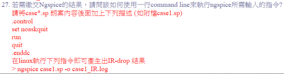
Q&A 27 => 介紹如何用ngspice command line 方式寫出IR-drop結果。 -
請問之後還會公佈新的測資嗎?還是case3是跟去年的一樣,學生可以自行下載使用?或是今年只有兩個測資
有case3即將公布。 -
每個testcase是否一定可以產生至少一個能符合ir-drop的解?學生現在在嘗試著解case3的問題時(程式解+手動解),盡可能最大化使用可繞線空間,但還是無法讓每個target都能過ir-drop,是否每個case一定可以至少產生一個解?亦或是有可能會有只有部分通過的情況?
因為case2已有隊伍可以全部達到IR-drop constraints,所以針對Case3, 我們出題的條件是 => 在達不到所有IR-drop constraints的情形之下,程式可以盡量完成PDN optimization,達到IR-drop constraints的比例越高越好,不可core dumped。 -
我想請問之後隱藏測資會有multi source的情況嗎?(例如像去年的case3)
會喔! -
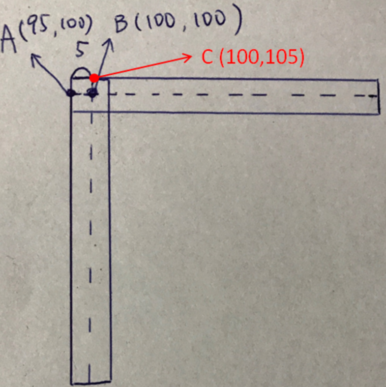
(1). 請問當我們換層時,兩條金屬線的線寬不同的話,(如下圖)是只需要放一個via就可以了,還是要放多個via呢?
(2).請問在sp檔中,若有轉彎處的線是要取下圖的A點還是B點作為座標點呢?
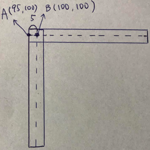
(1)如題目中Physical guideline:第五點提到,可以只放一個via,或在空間允許下放多個via(可並聯降低電阻值,Q&A 28亦有提到)
(2)sp檔裡面沒有描述座標,只有各線段電阻值的描述,如果是指def 以及R值的計算,則都是以A(95,100) 以及C(100,105)為起始點或終點來計算,如下圖。
-
因為官方給的VIA本身已經有包覆上下兩層的金屬了,我們在試DRC的過程中,沒有完全包覆VIA還是能通過DRC,請問這樣還需要將VIA全部包覆起來嗎?(如圖DRC是有通過的)
可以通過DRC,是因為現有DRC rule不夠齊備,如同FAQ 29,請參照題目中 Physical guideline的第五點,metal需完整的包覆via才符合規範。